標題: Titlebook: Contactless VLSI Measurement and Testing Techniques; Selahattin Sayil Book 2018 Springer International Publishing AG 2018 Integrated Circu [打印本頁] 作者: Suture 時間: 2025-3-21 17:37
書目名稱Contactless VLSI Measurement and Testing Techniques影響因子(影響力)
書目名稱Contactless VLSI Measurement and Testing Techniques影響因子(影響力)學科排名
書目名稱Contactless VLSI Measurement and Testing Techniques網絡公開度
書目名稱Contactless VLSI Measurement and Testing Techniques網絡公開度學科排名
書目名稱Contactless VLSI Measurement and Testing Techniques被引頻次
書目名稱Contactless VLSI Measurement and Testing Techniques被引頻次學科排名
書目名稱Contactless VLSI Measurement and Testing Techniques年度引用
書目名稱Contactless VLSI Measurement and Testing Techniques年度引用學科排名
書目名稱Contactless VLSI Measurement and Testing Techniques讀者反饋
書目名稱Contactless VLSI Measurement and Testing Techniques讀者反饋學科排名
作者: remission 時間: 2025-3-21 22:11
Probing Techniques Based on Light Emission from Chip,om off-state leakage) technique observes the near-infrared light emission associated with the off-state leakage of transistor. Since the emission is brighter for an NMOS transistor compared to a PMOS, this information is used to detect logic states. Finally, a technique based on the integration of a作者: Outmoded 時間: 2025-3-22 01:11
Contactless VLSI Measurement and Testing Techniques作者: FAZE 時間: 2025-3-22 04:50
Contactless VLSI Measurement and Testing Techniques978-3-319-69673-7作者: travail 時間: 2025-3-22 10:16 作者: Harass 時間: 2025-3-22 13:20 作者: Harass 時間: 2025-3-22 17:47 作者: inflate 時間: 2025-3-22 22:45 作者: 易發(fā)怒 時間: 2025-3-23 03:53
https://doi.org/10.1007/978-3-662-22587-5ntegrated circuits. This technique uses an electron beam to stimulate secondary electron emission from metallized surfaces. It uses the energy distribution function of the released secondary electrons which is in turn a function of the voltage at the test point. A very attractive feature of EBT is t作者: Affirm 時間: 2025-3-23 09:35 作者: 無禮回復 時間: 2025-3-23 10:16 作者: 縮短 時間: 2025-3-23 15:41 作者: 裂隙 時間: 2025-3-23 19:32
https://doi.org/10.1007/978-3-662-24751-8 is completely compatible with standard silicon IC processing. It uses optical signals transmitted to the circuit for “inputting” the stimulus data and also uses optical signals from the circuit for observation of the logic output. In addition, this approach is fully compatible with the simultaneous作者: Graphite 時間: 2025-3-24 00:02 作者: Charlatan 時間: 2025-3-24 02:58 作者: 戰(zhàn)役 時間: 2025-3-24 08:19 作者: 偽書 時間: 2025-3-24 11:24 作者: BIAS 時間: 2025-3-24 15:25
978-3-319-88819-4Springer International Publishing AG 2018作者: 場所 時間: 2025-3-24 23:04 作者: 密碼 時間: 2025-3-25 01:21
Comparison of Contactless Testing Methodologies,ss testing methodologies that covered in this text and makes a comparison based on above properties. This will be valuable to readers as contactless probing is gaining more importance as fabrication technologies become smaller and more susceptible to the parasitic impact of mechanical probes.作者: Immunoglobulin 時間: 2025-3-25 05:21 作者: Fluctuate 時間: 2025-3-25 07:39
lve many of the challenges associated with conventional mechanical wafer testing. The techniques described in this book address the increasing demands for internal access of the logic state of a node within a chip under test..978-3-319-88819-4978-3-319-69673-7作者: 強制令 時間: 2025-3-25 13:36 作者: 愛國者 時間: 2025-3-25 18:58 作者: 沉積物 時間: 2025-3-25 22:34 作者: 躲債 時間: 2025-3-26 03:44 作者: 課程 時間: 2025-3-26 05:52
us optical contactless testing techniques, such as Electro-O.This book provides readers with a comprehensive overview of the state-of-the-art in optical contactless probing approaches, in order to fill a gap in the literature on VLSI Testing.? The author highlights the inherent difficulties encounte作者: restrain 時間: 2025-3-26 10:31 作者: CLAMP 時間: 2025-3-26 13:20
https://doi.org/10.1007/978-3-662-22585-1growing portion of a product’s total costs. DFT techniques are valuable methods for helping solve the growing test problem. The cost is the increased silicon circuit area to accommodate the hardware overhead and potentially reduced circuit performance.作者: GET 時間: 2025-3-26 18:53 作者: endarterectomy 時間: 2025-3-26 22:08 作者: 確定無疑 時間: 2025-3-27 01:18
https://doi.org/10.1007/978-3-662-22587-5st industrially developed contactless testing technique. The photoemissive probe, on the other hand, uses a pulsed optical beam of a certain energy to probe a signal on a metal line of any substrate. The optical beam causes photoelectrons to be emitted from the top layer of a metal from which the waveform of the signal is derived.作者: 結束 時間: 2025-3-27 05:39
Contactless Testing,ing and design verification, as well as for functional testing. After some introduction on contactless testing, this chapter focuses on the photoexcitation probe technique. This technique uses a focused laser beam to photoexcite carriers near an active device to detect logic levels of transistors.作者: Graduated 時間: 2025-3-27 13:02 作者: 休息 時間: 2025-3-27 16:46
Conventional Test Methods,l and internal fault testing face increasingly difficult challenges. This chapter discusses these limitations of conventional methods and highlights the importance of alternative probing solutions to address the upcoming challenges.作者: Forsake 時間: 2025-3-27 18:20
Testability Design,growing portion of a product’s total costs. DFT techniques are valuable methods for helping solve the growing test problem. The cost is the increased silicon circuit area to accommodate the hardware overhead and potentially reduced circuit performance.作者: 惡臭 時間: 2025-3-27 22:42 作者: expdient 時間: 2025-3-28 02:52 作者: nocturia 時間: 2025-3-28 09:44 作者: 拔出 時間: 2025-3-28 13:00
https://doi.org/10.1007/978-3-662-24781-5ss testing methodologies that covered in this text and makes a comparison based on above properties. This will be valuable to readers as contactless probing is gaining more importance as fabrication technologies become smaller and more susceptible to the parasitic impact of mechanical probes.作者: insolence 時間: 2025-3-28 17:05 作者: 瑪瑙 時間: 2025-3-28 21:45 作者: Anal-Canal 時間: 2025-3-29 01:43
Other Techniques Based on the Contacting Probe,uctural or defect-based testing techniques. A functional test applies predetermined set of patterns at the inputs of an integrated circuit and compares to the expected responses. The goal is to verify the functionality of the chip under test. Structural tests, on the other hand, target on the defect作者: Directed 時間: 2025-3-29 03:09 作者: Bureaucracy 時間: 2025-3-29 10:23
Electron Beam and Photoemission Probing,ntegrated circuits. This technique uses an electron beam to stimulate secondary electron emission from metallized surfaces. It uses the energy distribution function of the released secondary electrons which is in turn a function of the voltage at the test point. A very attractive feature of EBT is t作者: 喊叫 時間: 2025-3-29 13:56 作者: 性滿足 時間: 2025-3-29 16:27
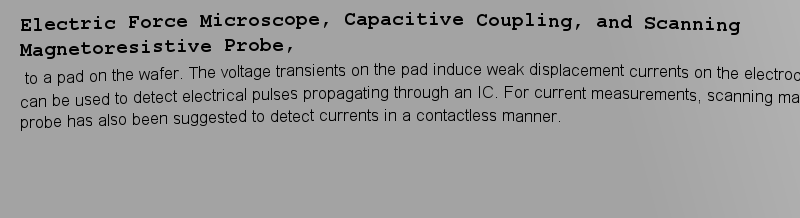
Electric Force Microscope, Capacitive Coupling, and Scanning Magnetoresistive Probe,connected line creates an electric force between the tip and the device under test which causes a detectable bending of the cantilever. This bending amount is optically detected and electrically analyzed by a lock-in amplifier. In capacitive coupling method, an electrode is placed in close proximity