標(biāo)題: Titlebook: Atomic Scale Interconnection Machines; Proceedings of the 1 Christian Joachim Conference proceedings 2012 Springer-Verlag Berlin Heidelberg [打印本頁(yè)] 作者: energy 時(shí)間: 2025-3-21 19:18
書(shū)目名稱Atomic Scale Interconnection Machines影響因子(影響力)
作者: NATTY 時(shí)間: 2025-3-21 20:34 作者: 孵卵器 時(shí)間: 2025-3-22 01:45 作者: 寬度 時(shí)間: 2025-3-22 07:34 作者: 顯示 時(shí)間: 2025-3-22 08:43 作者: 侵略 時(shí)間: 2025-3-22 15:07 作者: Employee 時(shí)間: 2025-3-22 20:34 作者: 過(guò)份 時(shí)間: 2025-3-23 00:34
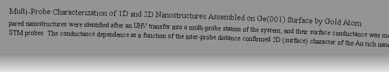
Christa Kleindienst-Cachay,Steffen Bahlkepared nanostructures were identified after an UHV transfer into a multi-probe station of the system, and their surface conductance was measured with two STM probes. The conductance dependence as a function of the inter-probe distance confirmed 2D (surface) character of the Au rich nanostructures ass作者: 織布機(jī) 時(shí)間: 2025-3-23 04:30 作者: 祝賀 時(shí)間: 2025-3-23 07:46
On the Road to Multi-Probe Non-Contact AFM,This contribution highlights some important aspects that have to be considered when building a multi-probe non-contact AFM. Specifically the requirements on the control system for such applications are considered.作者: 刺耳 時(shí)間: 2025-3-23 13:05 作者: inspiration 時(shí)間: 2025-3-23 17:23 作者: 仲裁者 時(shí)間: 2025-3-23 20:54
Christian JoachimAddresses for the first time multi-probes (multi-channels) atomically precise interconnections to an atom circuit or to a single molecule circuit.Includes supplementary material: 作者: 朋黨派系 時(shí)間: 2025-3-23 23:41 作者: 偶像 時(shí)間: 2025-3-24 02:56
https://doi.org/10.1007/978-3-642-28172-3AtMol; Atom Technology; LT-UHV STM; Molecule logic gates; Nano interconnections作者: 間諜活動(dòng) 時(shí)間: 2025-3-24 08:11
978-3-662-50821-3Springer-Verlag Berlin Heidelberg 2012作者: 有害 時(shí)間: 2025-3-24 13:49
Atomic Scale Interconnection Machines978-3-642-28172-3Series ISSN 2193-9691 Series E-ISSN 2193-9705 作者: 無(wú)節(jié)奏 時(shí)間: 2025-3-24 18:53 作者: 伴隨而來(lái) 時(shí)間: 2025-3-24 23:01 作者: 冰河期 時(shí)間: 2025-3-25 00:16
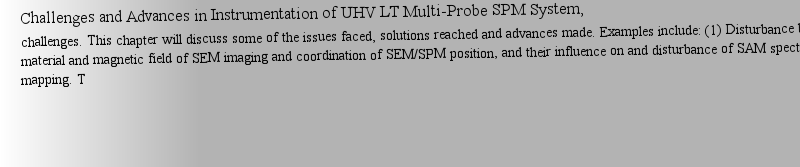
L O K - Das Wunder von Leipzig?,nd therefore functional devices are rare. The individual metallic contact interface represents one of the main challenges and high precision local electrical probing has the potential to increase efficiency in evaluating different approaches. To meet the involved requirements, we have established an作者: 包庇 時(shí)間: 2025-3-25 03:50
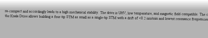
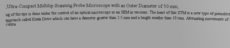
ng of the tips is done under the control of an optical microscope or an SEM in vacuum. The heart of this STM is a new type of piezoelectric coarse approach called Koala Drive which can have a diameter greater than 2.5?mm and a length smaller than 10?mm. Alternating movements of springs move a centra作者: 失眠癥 時(shí)間: 2025-3-25 09:25
r fabrication and surface analysis. The characterization part consists of low temperature scanning tunneling microscope (LT-STM), four probes variable temperature scanning tunneling microscope (Multiprobe), high resolution scanning electron microscope (SEM). The fabrication part has field ion micros作者: optional 時(shí)間: 2025-3-25 15:23 作者: HAWK 時(shí)間: 2025-3-25 16:57 作者: 收藏品 時(shí)間: 2025-3-25 22:18
Der brasilianische Fu?ball bis zur WM 2014 can arrange the atoms the way we want” (Feynman, “There’s Plenty of Room at the Bottom”, speech on December 29th . at the annual meeting of the American Physical Society at the California Institute of Technology). Twenty years ago, Don Eigler of IBM, did arrange atoms the way he wanted (Eigler and 作者: Tidious 時(shí)間: 2025-3-26 00:59 作者: ANTIC 時(shí)間: 2025-3-26 07:02
Christa Kleindienst-Cachay,Steffen Bahlkedevices. Local electrical contacts, namely nanoelectrodes, are often fabricated by using top-down lithography and chemical etching techniques. These processes however lack atomic precision and introduce the possibility of contamination. Here, we review recent reports on the application of a field-in作者: Malleable 時(shí)間: 2025-3-26 09:25 作者: NIP 時(shí)間: 2025-3-26 16:19 作者: Blazon 時(shí)間: 2025-3-26 17:53
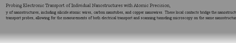
Kerstin P??iger,S?hnke Vosgerau with metal-coated carbon nanotube (CNT) tips. We first present our custom-made apparatus (with UNISOKU Co.) as well as CNT tips, and then some case studies with two different samples, Co-silicide nanowires self-assembled on Si(110) surface and Cu nanowires made by damascene processes used in LSI in作者: glomeruli 時(shí)間: 2025-3-26 22:24
Kerstin P??iger,S?hnke VosgerauSi(111)-1?×?1 surfaces. Metallic contacts with points spaced?<1?μm, deposited via electron-beam lithography, were used as contact points for two probes, while a central STM tip imaged the region between the contacts. A novel imaging method measuring the fraction of the tunneling current flowing to e作者: CAMP 時(shí)間: 2025-3-27 01:30 作者: 模范 時(shí)間: 2025-3-27 08:55
Kerstin P??iger,S?hnke Vosgeraut configurations will be discussed. The lateral transport of electrons may be studied by using two tips to drive a current parallel to the surface. A third tip enables to map the corresponding electrochemical potential ... Measurements for a 2D conducting layer will be discussed. To analyze the tran作者: 性別 時(shí)間: 2025-3-27 11:21 作者: ANIM 時(shí)間: 2025-3-27 16:19
,Ergebnisse der Studie im L?ngsschnitt, construction of complex devices at single molecular scale. In this chapter, two different kinds of single molecular motors at surfaces are studied with scanning tunneling microscopy (STM) technique. We discuss the structural and conductance transitions of one H2 rotaxane molecule at the sub-rotaxan作者: 障礙 時(shí)間: 2025-3-27 20:22 作者: Gastric 時(shí)間: 2025-3-27 22:42 作者: plasma-cells 時(shí)間: 2025-3-28 02:21 作者: NUDGE 時(shí)間: 2025-3-28 09:00
The DUF Project: A UHV Factory for Multi-Interconnection of a Molecule Logic Gates on Insulating Su) on insulating substrates are presented. In the Nanoscience group of Toulouse, the UHV factory has been developed since ten?years in order to realize under UHV the five levels of interconnections on insulating substrate, to characterize by NC-AFM the different steps and to measure the electrical pr作者: harmony 時(shí)間: 2025-3-28 12:33 作者: 過(guò)分 時(shí)間: 2025-3-28 15:22
Atomically Precise Manufacturing: The Opportunity, Challenges, and Impact, can arrange the atoms the way we want” (Feynman, “There’s Plenty of Room at the Bottom”, speech on December 29th . at the annual meeting of the American Physical Society at the California Institute of Technology). Twenty years ago, Don Eigler of IBM, did arrange atoms the way he wanted (Eigler and 作者: acetylcholine 時(shí)間: 2025-3-28 21:03 作者: 蠟燭 時(shí)間: 2025-3-29 00:09 作者: 令人不快 時(shí)間: 2025-3-29 03:11 作者: AUGUR 時(shí)間: 2025-3-29 11:10
Multi-Probe Characterization of 1D and 2D Nanostructures Assembled on Ge(001) Surface by Gold Atom and conductive mesa pads as components in electronic circuits. For such applications, we need a good knowledge of structural and electronic properties of 1D and 2D conductive nanostructures fabricated on large and/or moderate band gap semiconductor surfaces. This chapter is reporting on case studie作者: 項(xiàng)目 時(shí)間: 2025-3-29 12:00 作者: 燒烤 時(shí)間: 2025-3-29 18:13
Silicon Surface Conductance Investigated Using a Multiple-Probe Scanning Tunneling Microscope,Si(111)-1?×?1 surfaces. Metallic contacts with points spaced?<1?μm, deposited via electron-beam lithography, were used as contact points for two probes, while a central STM tip imaged the region between the contacts. A novel imaging method measuring the fraction of the tunneling current flowing to e作者: BILK 時(shí)間: 2025-3-29 21:28 作者: SEMI 時(shí)間: 2025-3-30 01:36 作者: Between 時(shí)間: 2025-3-30 05:42
Solid State Nano Gears Manipulations,h vacuum (UHV) scanning tunneling microscopy (STM) are used to maneuver the gears. The aim is to bridge the gap between the current solid state gears and the now available nanoscale gears. As in many technology integrations, miniaturization is a way to boost efficiency and an opening to new applicat作者: 高興去去 時(shí)間: 2025-3-30 10:02
Probing Single Molecular Motors on Solid Surface, construction of complex devices at single molecular scale. In this chapter, two different kinds of single molecular motors at surfaces are studied with scanning tunneling microscopy (STM) technique. We discuss the structural and conductance transitions of one H2 rotaxane molecule at the sub-rotaxan作者: 有偏見(jiàn) 時(shí)間: 2025-3-30 14:33
2193-9691 rcuit.Includes supplementary material: This volume documents the first International Workshop on Atomic Scale Interconnection Machines organised by the European Integrated Project AtMol in June 2011 in Singapore. The four sessions, discussed here in revised contributions by high level speakers, span作者: 淺灘 時(shí)間: 2025-3-30 18:04
L O K - Das Wunder von Leipzig?,ctrical probing has the potential to increase efficiency in evaluating different approaches. To meet the involved requirements, we have established and being advancing an approach for nano-scale electrical probing at low temperatures by integrating scanned probe microscopic (SPM) technology with high resolution electron microscopy.作者: glans-penis 時(shí)間: 2025-3-30 23:46
temperature scanning tunneling microscope (Multiprobe), high resolution scanning electron microscope (SEM). The fabrication part has field ion microscope (FIM), evaporators and nanoimprinter. The characteristics of every part of the instrument and the preliminary experiments on Si(100) surface are discussed.作者: 進(jìn)步 時(shí)間: 2025-3-31 00:57
Fu?ballfans als politische Akteur*innenthat operates under a scanning electron microscope in ultra-high vacuum and fulfills these requirements thanks to a unique control system. We show how this instrument is well adapted to study the resistivity of semiconductor nanowires.作者: 反饋 時(shí)間: 2025-3-31 08:41
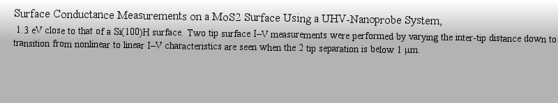
Christa Kleindienst-Cachay,Steffen Bahlke 1.3?eV close to that of a Si(100)H surface. Two tip surface I–V measurements were performed by varying the inter-tip distance down to 100?nm. A transition from nonlinear to linear I–V characteristics are seen when the 2 tip separation is below 1?μm.作者: STALE 時(shí)間: 2025-3-31 10:39
Kerstin P??iger,S?hnke Vosgerautudies with two different samples, Co-silicide nanowires self-assembled on Si(110) surface and Cu nanowires made by damascene processes used in LSI industry. It is shown that the four-tip STM with CNT tips is versatile and powerful for measuring the conductivity of individual nanostructures.作者: HUMP 時(shí)間: 2025-3-31 14:16
High Precision Local Electrical Probing: Potential and Limitations for the Analysis of Nanocontactsctrical probing has the potential to increase efficiency in evaluating different approaches. To meet the involved requirements, we have established and being advancing an approach for nano-scale electrical probing at low temperatures by integrating scanned probe microscopic (SPM) technology with high resolution electron microscopy.作者: Kinetic 時(shí)間: 2025-3-31 18:54 作者: gerontocracy 時(shí)間: 2025-3-31 23:33
Combined STM and Four-Probe Resistivity Measurements on Single Semiconductor Nanowires,that operates under a scanning electron microscope in ultra-high vacuum and fulfills these requirements thanks to a unique control system. We show how this instrument is well adapted to study the resistivity of semiconductor nanowires.作者: LINES 時(shí)間: 2025-4-1 01:54 作者: MIR 時(shí)間: 2025-4-1 07:49
Nanometer-Scale Four-Point Probe Resistance Measurements of Individual Nanowires by Four-Tip STM,tudies with two different samples, Co-silicide nanowires self-assembled on Si(110) surface and Cu nanowires made by damascene processes used in LSI industry. It is shown that the four-tip STM with CNT tips is versatile and powerful for measuring the conductivity of individual nanostructures.