作者: IOTA 時(shí)間: 2025-3-21 23:25
Expanding the Economic Concept of Exchangemeters. Module frequencies of operation range from typical values of approximately 60 MHz for low-end digital applications to multi-gigahertz rf applications. Operating frequency is a primary socket design factor since it has a significant influence on the module contacting method.作者: Cleave 時(shí)間: 2025-3-22 04:02 作者: indoctrinate 時(shí)間: 2025-3-22 04:37
Schriften zur Unternehmensentwicklungout advanced thin-film wiring. Thin-film wiring provides the highest level of wiring for both Single Chip Modules (SCM) and Multi-chip Modules (MCM). Relative comparisons are also made for availability, cost, characteristics and various application form factors.作者: 相容 時(shí)間: 2025-3-22 11:05 作者: AWE 時(shí)間: 2025-3-22 15:52 作者: 泥沼 時(shí)間: 2025-3-22 18:02
Ceramic Chip Carriersout advanced thin-film wiring. Thin-film wiring provides the highest level of wiring for both Single Chip Modules (SCM) and Multi-chip Modules (MCM). Relative comparisons are also made for availability, cost, characteristics and various application form factors.作者: Terminal 時(shí)間: 2025-3-22 23:02
Laminate/HDI Die Carriersey all allow the designer to significantly increase routing density through the use of vias in SMT pads, to reduce size and weight of product, and to improve the electrical performance of the system. These types of boards are generically called, . or ..作者: 壓倒性勝利 時(shí)間: 2025-3-23 04:13 作者: mitten 時(shí)間: 2025-3-23 08:19 作者: 口訣法 時(shí)間: 2025-3-23 12:06
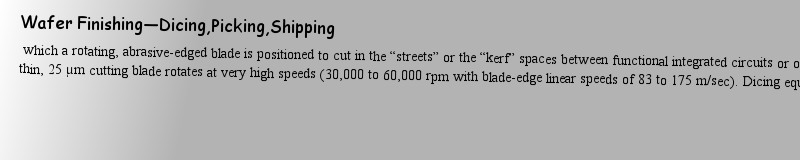
https://doi.org/10.1007/978-3-658-23316-7her precision, greater throughput and reduced damage to the topside and bottom-side edges of the dice. In this chapter, the reader is introduced to the dicing process and made aware of the key issues which must be considered when setting up a die separation process [1, 2].作者: pulmonary-edema 時(shí)間: 2025-3-23 15:11 作者: 躲債 時(shí)間: 2025-3-23 18:16 作者: Certainty 時(shí)間: 2025-3-24 01:59
Wafer Bumping judgements or critiques as to what is good or bad. The marketplace is expected to be the ultimate sorting place which will accept some of the best, and reject others which fall short due to cost, manufacturability, reliability or functionality.作者: 破裂 時(shí)間: 2025-3-24 02:32
Wafer Finishing—Dicing,Picking,Shippingher precision, greater throughput and reduced damage to the topside and bottom-side edges of the dice. In this chapter, the reader is introduced to the dicing process and made aware of the key issues which must be considered when setting up a die separation process [1, 2].作者: 天真 時(shí)間: 2025-3-24 10:18
Reliability of Die-Level Interconnectionsthe field can be predicted on the basis of short term tests. The validity of the tests is achieved by verifying established semi-empirical models and characteristic parameters, and then are employed to predict the field life of joints.作者: MARS 時(shí)間: 2025-3-24 13:13
Ceramic Ball and Column Grid Arrayskage structure descriptions, range of offerings, established infrastructure and performance attributes. Package interconnection processes are discussed in detail, as are the benefits derived from these packages, as illustrated through several example applications.作者: 因無(wú)茶而冷淡 時(shí)間: 2025-3-24 16:47
ed in the last third of the twentieth century. Packaging has provided the necessary external wiring and interconnection capability for transistors and integrated circuits while they have gone through their own spectacular revolution from discrete device to gigascale integration. At IBM we are proud 作者: 無(wú)法破譯 時(shí)間: 2025-3-24 21:26 作者: 摘要記錄 時(shí)間: 2025-3-24 23:56
Underfill: The Enabling Technology for Flip-Chip Packagingny reinforcement [1]; the use of a polymeric material to surround the solder connections beneath attached chips has allowed flip chips with large die footprints and increased neutral point distances to be utilized even with organic chip carriers.作者: milligram 時(shí)間: 2025-3-25 03:22
https://doi.org/10.1007/978-3-658-23316-7Wire bonds, tape automated bonding (TAB), and solder-bump, flip-chip connections more popularly referred to as controlled collapsed chip connections or C4 are the three primary chip-to-carrier interconnection technologies currently practiced.作者: 重疊 時(shí)間: 2025-3-25 07:55
Expanding the Economic Concept of ExchangeThe industry has focused on replacing packaged chips such as pin-in-hole (PIH) and surface-mount components (SMT) on cards or boards. Components which do not pass electrical test or inspection are removed from cards but not chips from single chip packages. In some instances, such as plastic molded packages, removal is not a viable option.作者: FLAIL 時(shí)間: 2025-3-25 12:00
Flip-Chip Die Attach TechnologyWire bonds, tape automated bonding (TAB), and solder-bump, flip-chip connections more popularly referred to as controlled collapsed chip connections or C4 are the three primary chip-to-carrier interconnection technologies currently practiced.作者: Mortal 時(shí)間: 2025-3-25 17:39 作者: 晚間 時(shí)間: 2025-3-25 21:42
https://doi.org/10.1007/978-1-4615-1389-6Potential; Scale; Wafer; development; interconnect; manufacturing; material; metal; climate change作者: 確定無(wú)疑 時(shí)間: 2025-3-26 04:01 作者: 過(guò)分 時(shí)間: 2025-3-26 06:25
http://image.papertrans.cn/b/image/161489.jpg作者: CANON 時(shí)間: 2025-3-26 10:02 作者: myriad 時(shí)間: 2025-3-26 12:47 作者: 嚴(yán)厲批評(píng) 時(shí)間: 2025-3-26 20:47 作者: Explosive 時(shí)間: 2025-3-26 21:39 作者: municipality 時(shí)間: 2025-3-27 03:42 作者: Lethargic 時(shí)間: 2025-3-27 09:07 作者: 撤退 時(shí)間: 2025-3-27 11:32 作者: 態(tài)度暖昧 時(shí)間: 2025-3-27 17:33 作者: anchor 時(shí)間: 2025-3-27 20:06
Expanding the Economic Concept of ExchangeM) and their corresponding socket form factors are described ranging from small chip scale packages (CSP) having micro ball grid arrays (MBGA) to very large land grid arrays (LGA) having in excess of 5000 I/Os [1]. Module sizes correspondingly range from tens of millimeters to over one hundred milli作者: 可能性 時(shí)間: 2025-3-27 23:20
Expanding the Economic Concept of Exchangeckaging. Although flip-chip interconnection, or controlled collapse chip connection (C4) as it is also known, has a long history prior to the use of any reinforcement [1]; the use of a polymeric material to surround the solder connections beneath attached chips has allowed flip chips with large die 作者: 輕浮女 時(shí)間: 2025-3-28 04:08
https://doi.org/10.1007/978-1-4615-0905-9tal migration, electromigration, creep, and thermomigration. Under normal field conditions, non-encapsulated open-array flip chip solder joints attached to alumina chip carriers exhibit the best reliability in the field among all interconnect methods. This, of course, is the result of following esta作者: filicide 時(shí)間: 2025-3-28 06:35
Stuart Cunningham,Peter S. Excellth increased speed and decreased energy consumption requirements has led to present day highly integrated circuits. To take advantage of the integration enhancements at the die level, much attention is focused on the supporting package performance.作者: gentle 時(shí)間: 2025-3-28 11:09 作者: Excise 時(shí)間: 2025-3-28 17:08
Pak Chung Wong,Han-Wei Shen,Chaomei Chennted circuit card or board. Previously this family of packages has been referred to by several designations, among them: Area Array Tape Automated Bonding (ATAB) [1], Tape Ball Grid Array (TBGA) [2], fleXBGA. [3], Wire Bond TBGA (WB TBGA) [4], Signetics TBGA (S-TBGA) [5], Flex TBGA (FTBGA) [6], Star作者: 高度 時(shí)間: 2025-3-28 20:58 作者: NAIVE 時(shí)間: 2025-3-29 00:10
https://doi.org/10.1057/9781137006004 input-output connections all over the face of a flip chip is also a simple idea, and twenty-five years old. Then, how is it, in the last days of the twentieth century, that the electronics industry finds itself in the midst of a revolution in electronic assembly referred to as flip-chip area-array packaging?作者: 主動(dòng) 時(shí)間: 2025-3-29 03:21 作者: 豐富 時(shí)間: 2025-3-29 07:23
Expanding the Economic Concept of Exchanget the productivity of a manufacturing plant span from initial package design to finished product inspection. As with any manufacturing operation, tradeoffs must be constantly evaluated to achieve an acceptable balance between quality, production, cost and reliability objectives.作者: obsolete 時(shí)間: 2025-3-29 13:21
Stuart Cunningham,Peter S. Excellth increased speed and decreased energy consumption requirements has led to present day highly integrated circuits. To take advantage of the integration enhancements at the die level, much attention is focused on the supporting package performance.作者: hankering 時(shí)間: 2025-3-29 16:21
https://doi.org/10.1007/978-1-4471-2804-5rate is a thin (less than 0.035 inches) laminate similar to card technologies used for personal computers. Although the interconnections between a chip and substrate are typically wire bonds, flip-chip dice can be attached to PBGA packages as well. PBGA technologies also support chip scale packaging (CSP) discussed in Chapters 18 and 23.作者: assent 時(shí)間: 2025-3-29 21:24
History of Flip Chip and Area Array Technology input-output connections all over the face of a flip chip is also a simple idea, and twenty-five years old. Then, how is it, in the last days of the twentieth century, that the electronics industry finds itself in the midst of a revolution in electronic assembly referred to as flip-chip area-array packaging?作者: exorbitant 時(shí)間: 2025-3-30 02:35 作者: 我悲傷 時(shí)間: 2025-3-30 07:56 作者: Ergots 時(shí)間: 2025-3-30 09:51
Ceramic and Plastic Pin Grid Array Technologyth increased speed and decreased energy consumption requirements has led to present day highly integrated circuits. To take advantage of the integration enhancements at the die level, much attention is focused on the supporting package performance.作者: 頭盔 時(shí)間: 2025-3-30 13:32 作者: ANIM 時(shí)間: 2025-3-30 16:55 作者: 誘惑 時(shí)間: 2025-3-30 21:16
Wafer Bumpinge are immediate questions which emerge: Who will put bumps on chips and how? Will the same bumped chips be joined to both ceramic and organic packages? Must all chips be joined with high-melting or low-melting solders, or not with solder at all, but with conductive adhesives? This chapter will illus作者: 合唱隊(duì) 時(shí)間: 2025-3-31 01:11 作者: neutrophils 時(shí)間: 2025-3-31 08:23 作者: packet 時(shí)間: 2025-3-31 10:15 作者: Tortuous 時(shí)間: 2025-3-31 15:48
Ceramic Chip Carriersic chip carrier examples for each of the six market applications which include High Performance, Cost Performance, Commodity, Hand Held and Communication, Automotive and Memory. Materials and properties are summarized for standard alumina chip carriers, high-performance materials, thin-film material作者: 戲法 時(shí)間: 2025-3-31 19:08